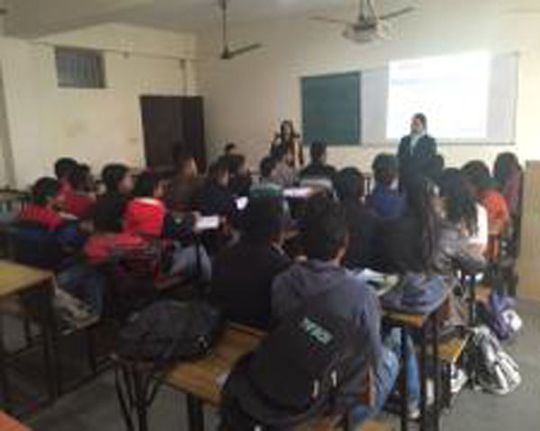
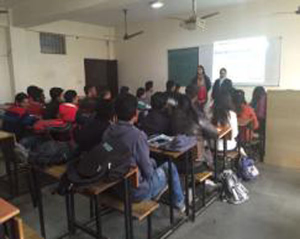
Electronics & Computer Engineering Department of Dronacharya College of Engineering, Gurgaon organized a week Winter School on VLSI Design from 18th - 22nd January 2016 at college campus. |
| |
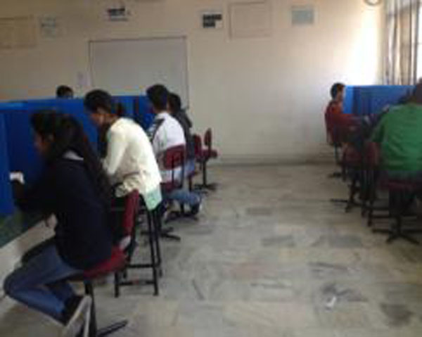
The objective of the Winter School was to groom and empower students to train them self - sufficient in the field of VLSI Design by giving them hands on Mircowind Tool and XILINX tool. The program was coordinated by Ms Seema, Ms Shakshi Pahuja, and Ms Priya Yadav from ECE and ECS department in which 19 students participated. |
| |
Day 1 : Monday, 18 January 16 |
| |
First day session was started with introduction of VLSI Design, Moores law and Gajaskis Y chart for basic understanding of modeling designs from structural domain to physical domain. Students were explained about block diagram, difference between front end and back end in the VLSI Design along with benefits of this course. |
| |
The practical session started with introduction to Micro wind tool in which CMOS Inverter was designed with help of PMOS inverter, NMOS inverter with timing waveform verification. |
| |
MICROWIND is truly integrated EDA software encompassing IC designs from concept to completion, enabling chip designers to design beyond their imagination. MICROWIND integrates traditionally separated front - end and back - end chip design into an integrated flow. |
| |
Day 2 : Tuesday, 19 January 16 |
| |
The second day session started with introduction on CMOS Design. CMOS (Complementary metal oxide semiconductor) is technology for constructing integrated circuits. It is used in microprocessors, microcontrollers, static RAM and other digital logic circuits. Students were briefed about fabrication processes like Oxidation, Photolithography, Etching, Metallization, PMOS fabrication process & layout. |
| |
In practical session PMOS inverter, NMOS inverter and timing waveform verification on DSCH3 was explained in Micro wind tool. |
| |
Day 3 : Wednesday, 20 January 16 |
| |
The third day session started with introduction to HDL (Hardware description language) Hardware Description Language (HDL) is a specialized computer language used to describe the structure and behavior of electronic circuits, and most commonly, digital logic circuits. Different levels of abstraction from algorithmic level to gate level was also explained and various gates were programmed using structural modeling style. |
| |
In practical session steps to install the XILINZ software and steps to write program & verify the waveforms were explained. Basic gates were programmed using XILINX tool and waveforms were verified in simulator. |
| |
Day 4 : Thursday, 21 January 16 |
| |
On fourth day , different styles of Modeling (structural, data flow and behavioral) was explained The student programmed the software on Half - Adder, Full - Adder, Half-Subtractor and Full - Subtractor with the help of structural , data flow and behavioral style of modeling. Different types Operator and Ports (Input, Output, and Inout) were also discussed in details. |
| |
During the practical session students programmed Adder, Subtractor, Multiplexer and Demuliplexer using XILINX tool and waveforms were verified in simulator. |
| |
Day 5 : Friday, 22 January 16 |
| |
On the last day, the session started with introducing ROM, RAM and PLA. PLD (Programmer Logic Devices), FPGAS, CPLD and ASIC were also explained in details. PLD is an electronic component used to build reconfigurable digital circuits. Through explanation students learned about difference between FPGAS (Field Programmable Gate Array) and CPLD (Complex Programmable Logic Device) and how synthesis becomes complete with burning of program in FPGA a CPLD kit. |
| |
In the practical session students verified their program on FPGA (Field Programmable Gate Array) and CPLD (Complex Programmable Logic Device) kit. They learnt about steps to configure kits with the system. |
| |
This Winter School on VLSI Design was helpful to students who were taking first step towards VLSI Design which groomed and empowered budding Engineers to become Self - sufficient in field of VLSI Design. |
| |
| |
| |
| |
| |
|
|
|
|
|
|
|
|
|
|
|
|
|
| |
|
|
|
| |
|
|
|
| |
|
|
|
| |
|
|
|
| |
|
|
|
| |
|
|
|
| |
|
|
|
| |
|
|
|
| |
|
|
|